| INA Resources | |
|---|---|
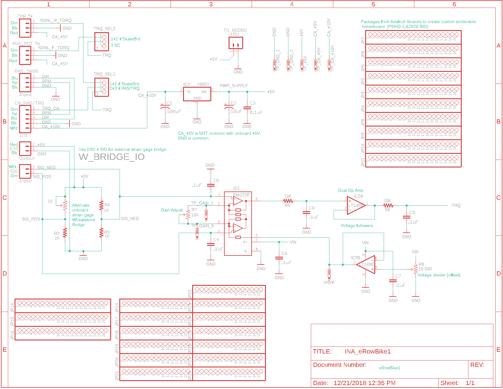
| INA Schematic | Current Reference schematic for Tringa INA |
| INA Connections | Reference for all connections/connectors to and from the INA. |
| Torque Handlebars | Reference for all connections/connectors to and from the handlebars, which act as the "torque sensor". |
| Instrumentation Amplifier IC | Documentation and notes on using the INA122 chip on our INA board. |
| INA122 Datasheet (PDF) | TI datasheet for the INA122 instrumentation amplifier IC. |
| Signal Inputs | Positive and Negative input signal lines coming from Wheatstone Bridge strain gages. |
| Gain Adjustment | Adjusting the gain on the INA122. |
| Reference Voltage | Setting the Reference Voltage on the INA122 using half of a dual op-amp IC. |
| LT1490 Dual Op-Amp | |
| Strain Gages | Documentation and resources for the strain gages we use on this project |
| Grin4 INA photo and schematic | Deep link into original ES thread! |
| Justin's eLongBoard development | This is the 'new' thread: "Grin's weight sensing electric longboards #4 and 5, and kit!" |
Because the original eRowBike1 design did not include PAS as part of its e-assist strategy, we began with a simpler (fewer inputs and outputs) strain gage amplifier circuit than Justin's "Grin4" INA circuit. We assumed that we'd obtain our torque signal from a Wheatstone bridge strain gage configuration that was attached to the handlebars and measured the deflection caused by the rider's backward pull. The amplifier module's output would be mapped into the 1-4VDC range, making it compatible with a typical ebike throttle. While this means that the INA could theoretically be used as the bike's "throttle," the reality is that the torque signal needs to be substantially smoothed to provide an acceptable ride. The addition of PAS data to the torque signal allows even more smoothing to be done by averaging the rider's effort over the entire rowing stroke.
We selected an Instrumentation Amplifier chip (INA122; Burr-Brown/TI) that only needed a single voltage (rail) input, and would allow sufficient gain and filtering to utilize the expected 4-5 millivolt (mV) signal coming from the strain gage array. Live testing various prototypes along the way made it clear that the BLDC motors we used create large amounts of electromagnetic interference (EMI) when running, so the INA's design incorporates methods to minimize the effects of the EMI.
We are currently (12/2018) working to include the PAS signals via a pickup unit mounted to the erowbike's power lever. The PAS effort, after an initial trial, has been placed on hold (June 2020).
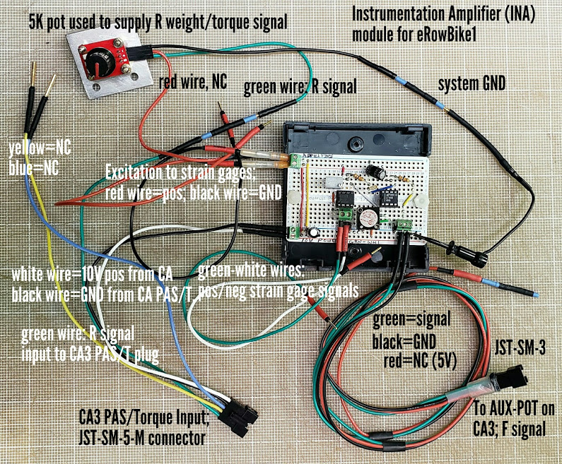
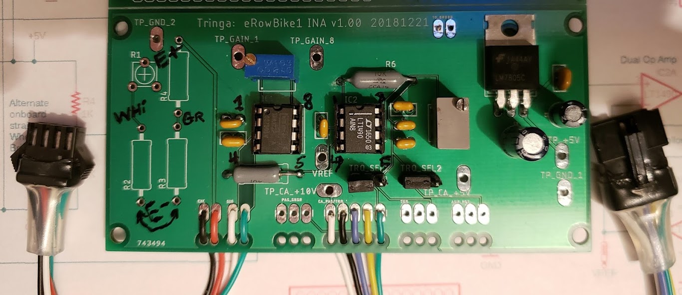
Connections and configuration for INA v1.0 20181221.
INA populated PCB for eRowBike1 [v1.0 20181221]
Note that in this photo the jumpers are in the "skateboard" firmware position.
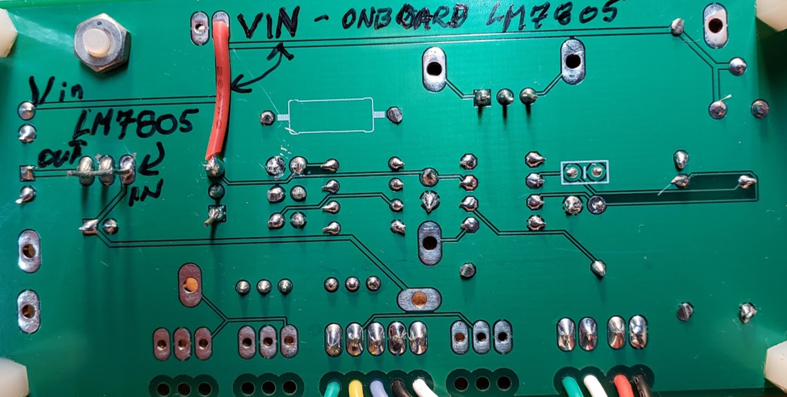
This is the second fully assembled board of the v1.0 20181221 version, showing the reverse (non-component) side. Note the red jumper wire (26AWG, silicone/stranded) connecting the two separated onboard 5V regulated Vin traces. The top end is attached to a Vin test point/solder pad while the other (bottom) end is connected to the input power pin of the reference voltage pot (both were convenient and solid soldering options). The Vin trace on the board goes from the pot to the power input pins of the IC's (pin #8 of the dual op-amp and pin #7 of the INA) via several intermediate filter caps. In something of an ongoing mystery [2 Oct 2020], the original schematic for this board didn't apparently provide any 5V power for either chip, although the first completed INA board, shown above, has been working fine on a prototype eRowbike1 for the past several years.
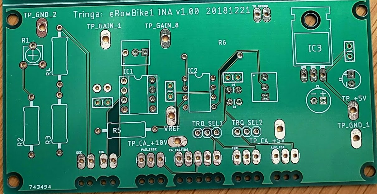
INA bare PCB for eRowBike1 [v1.0 20181221]
Current (Eagle) INA board schematic for eRowBike1 [v1.0 20181221]; Link is: http://erowbike.com/pics/INA122_instrumentation_amplifier_eagle_schematic.png
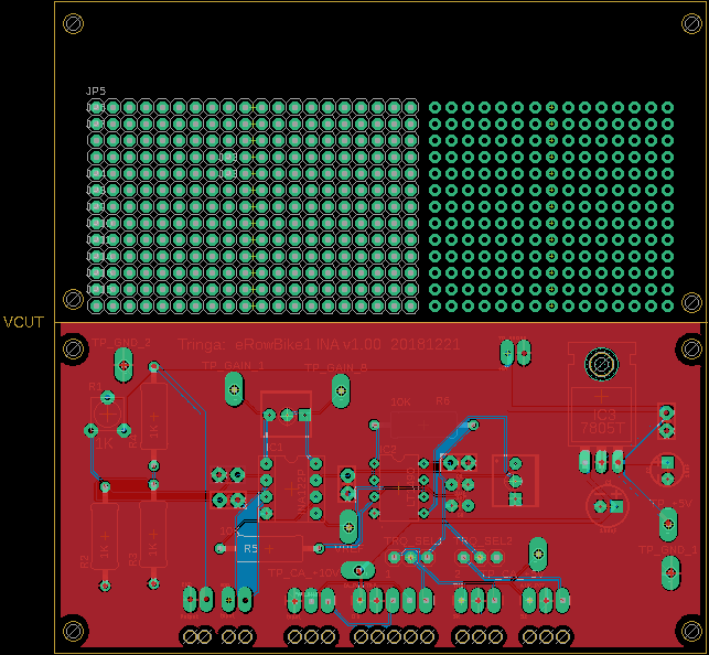
Current (Eagle) INA board layout for eRowBike1 [v1.0 20181221]
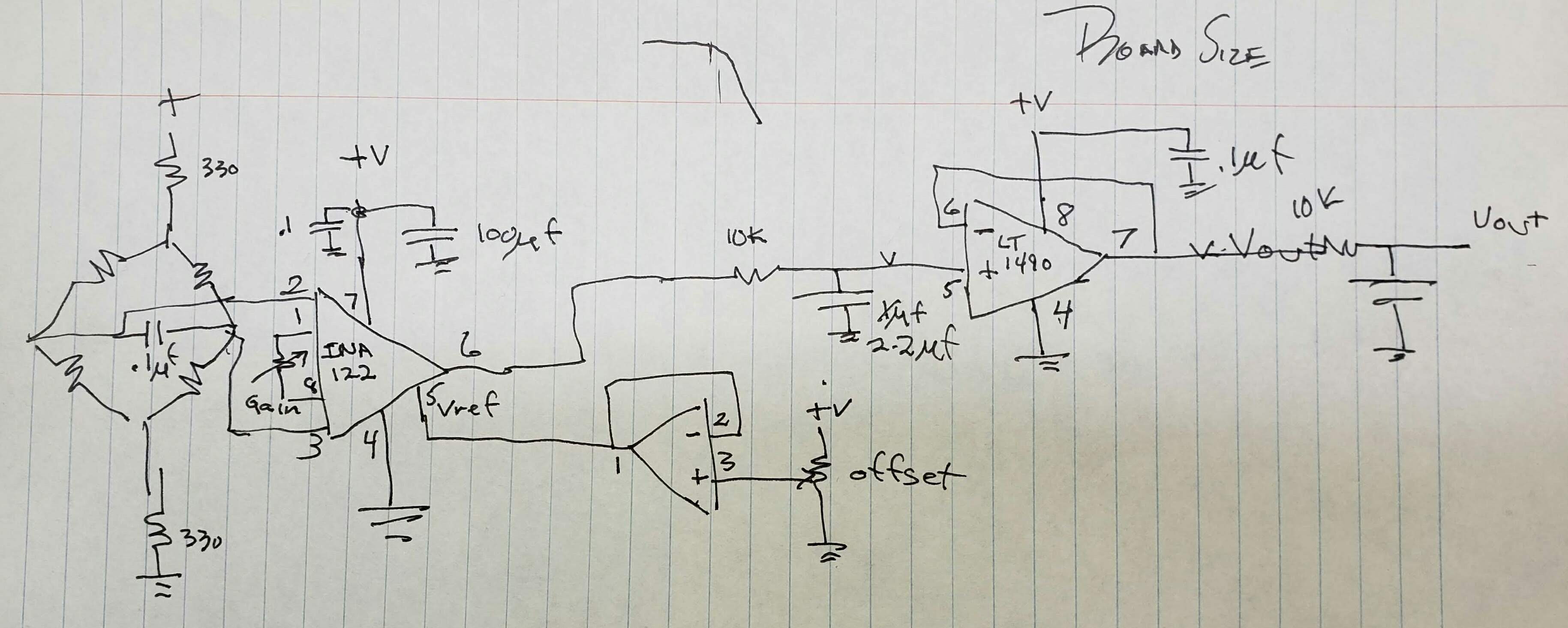
Original hand-drawn INA board schematic for eRowBike1 (Denny Fox, 2017; pen and paper).
Justin says that the 10V supplied by the CA (via the PAS/TORQ connector) is not regulated, and that I should use a 5V regulator chip on the INA to supply a stable voltage supply for the strain gage bridge excitation, the instrumentation amplifier, and the support chips. This has been done as of version 1.0 20181221.
Prototype (soldered breadboard) INA board used on eRowBike1
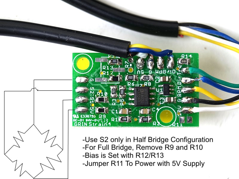
The following photo shows Justin's "Grin4" Instrumentation Amplifier board with a Wheatstone configured strain gage inputs. Tringa modeled its INA board on the functionality of the Grin4 board -- thanks Justin!
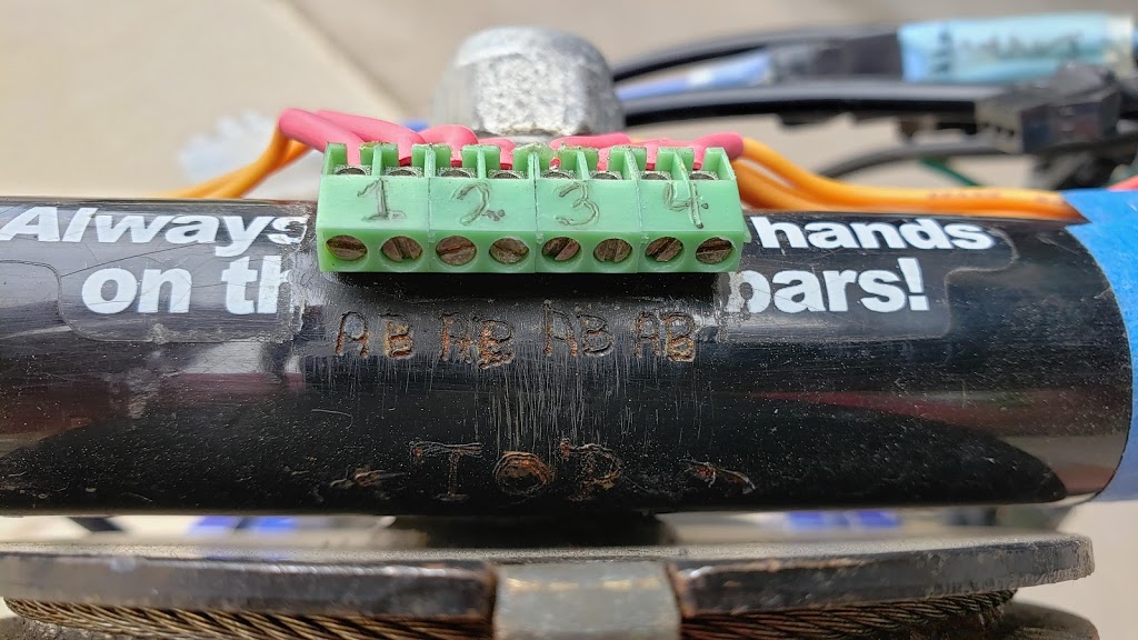
The following closeup shows the 'combiner' terminal strip used to connect to each of the four strain gages (orange wires) mounted on the handlebars in a Wheatstone Bridge configuration. This corresponds to the "1 2 3 4" markings on the terminal strip. Each strain gage has two connections, resulting in the total of eight separate terminals on the strip. This corresponds to the "AB" engraved into the metal handlebars (e.g., 1A, 1B, 2A, etc.).
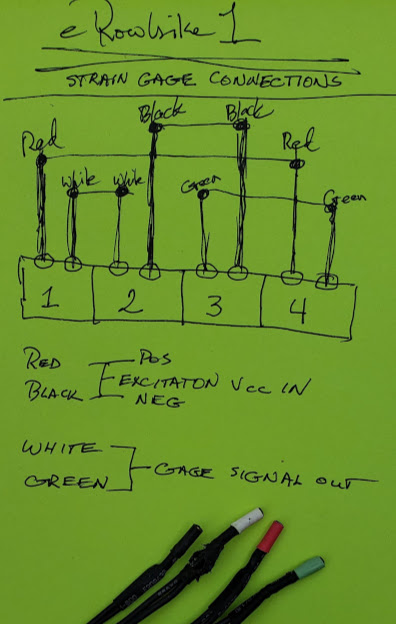
The INA board 'sees' the four separate strain gauges on the handlebars as a single, standard 'load cell' with only four connections. Two are for the 5V (plus and minus) excitation current, and two are for the combined strain gages signal output (white and green). Think of the handlebars as simply being a digital scale. See INA122 Signal Inputs for a more detailed explanation of how this works.
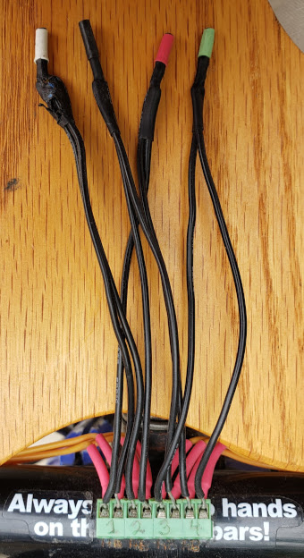
The following photo shows the the wires that effectively combine the 8 individual strain gage connections to the 4 INA connections. Notice the damage to one of the strain gage signal wires (white band) resulting from sliding the bike in and out of a Tesla Model S. After repair, we'll add some protection against physical and weather damage now that we know this layout works.
The hand-drawn schematic below shows how the 8 terminals of the individual 4 strain gages are combined for the INA board's 4 connections.
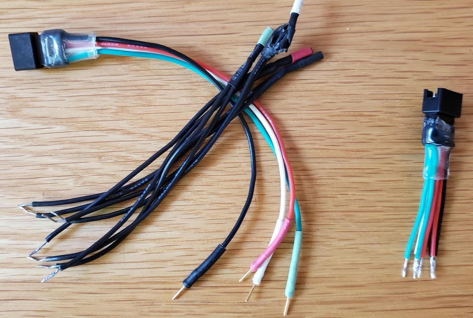
The damage to the original wiring presented an opportunity to shorten and simplify the connector. The new wiring (on the right side of the photo below) uses a single JST-SM-4M connector in which each of the 4 signal lines for the INA input is split into two separate pigtails to connect to the 8 pin 'combiner' terminal. In future versions it would make sense to wire the entire Wheatstone Bridge load cell handlebars so that only the four wires (2 for excitation and 2 for the analog torque signal) were visible to begin with. The handlebars should be an environmentally hardened and interchangeable unit to make maintenance easier.
The actual "instrumentation amplifier" (INA) integrated circuit ("IC") chip is the brain, heart, and soul of the INA board. Everything else on the board is basically 'support circuitry' to enable the INA IC to do its thing.
Per the TI (Burr-Brown/TI) datasheet https://www.ti.com/lit/ds/symlink/ina122.pdf:
"The INA122 is a precision instrumentation amplifier for accurate, low noise differential signal acquisition. Its two-op-amp design provides excellent performance with very low quiescent current, and is ideal for portable instrumentation and data acquisition systems. The INA122 can be operated with single power supplies from 2.2V to 36V and quiescent current is a mere 60µA. It can also be operated from dual supplies. By utilizing an input level-shift network, input common-mode range extends to 0.1V below negative rail (single supply ground). A single external resistor sets gain from 5V/V to 10000V/V. Laser trimming provides very low offset voltage (250µV max), offset voltage drift (3µV/°C max) and excellent common-mode rejection. Package options include 8-pin plastic DIP and SO-8 surface-mount packages. Both are specified for the -40°C to +85°C extended industrial temperature range."
On our original breadboard prototype board, we used the CA's available PAS 10V supply directly to drive our INA board's components. We used two inline 300 ohm resistors to drop the excitation voltage going to the strain gages to somewhat less than 5V, one resistor on the positive and one on the negative lines. For future developments, Justin suggested using an onboard 5V voltage regulator since the CA's 10V was not regulated or protected, and that the 5 volts was just a more preferred voltage.
We now take the CA's 10V output (white/pos and black/gnd wires on CA-PAS plug) and supply a LM7805 linear voltage regulator sub-circuit on the INA board to produce a clean 5V to drive not only the strain gages but also the remainder of the onboard circuits. All this is well within the INA122's 2.2 to 36 volt operating range.
An instrumentation amplifier takes as its INputs (on pins #2 and #3) two voltages, and OUTputs (on pin #6) the DIFFERENCE between the two input voltages, MULTIPLIED (amplified) by some user selectable GAIN factor.
On our INA board, the INA122's inputs come from four separate 350 ohm strain gages located on the eRowBike1's handlebars. They are wired together in what is known as a "Wheatstone bridge" configuration, resulting in two wires going into the bridge and two coming out. This method of connection makes the strain gages extremely sensitive to the rider's pushing and pulling the handlebars, and also resistant to environmental distractions such as temperature changes. This configuration is often referred to as a 'standard resistive bridge device' or 'load cell'.
When the user pulls on the handlebars -- regardless of what the handlebars are attached to -- the handlebars flex very slightly, and this deflection is accurately measured by the strain gages ("bridge"). For this to work, the bridge must be "excited" (not "exited") by some voltage to force the electrons to flow through it. When excited, the bridge's output will vary up and down proportionally over a very small voltage range (typically less than 10 millivolts) as the handlebars are pulled and pushed. The voltage on one bridge output wire will be higher relative to the other, so we refer to it as the 'positive' signal, although this matters only in the context of what we do with it. We arbitrarily use a green wire for the 'positive' signal and a white wire for the 'negative'.
You can also think of the bridge's two output wire signals as a single voltage (potential) when measured *between* them, as opposed to each signal wire's potential above the ground signal. Either way, the bridge's positive output (green wire) goes to input pin #2 on the INA122 while the bridge's negative output (white wire) goes to the INA122 input pin #3.
edit CMV...sitting 'on top of' a "common mode" voltage (CMV).
The CMV is what's left of the +5V excitation voltage being dissipated by the tiny wires in the strain gauges. The strain gages are nothing more than resistors whose resistance changes ever so slightly when they are flexed.
For such a device when "balanced" -- neither pushed nor pulled -- the CMV at either of the bridge's outputs will be half the supply (excitation) voltage. Remember that this voltage potential exists between each signal wire and ground, NOT between the two signal wires (which should be zero volts when the bridge is balanced). As we are "exciting" the bridge with +5V, the CMV will be about 2.5 volts. The CMV will be higher if the excitation voltage is higher (e.g., 10 volts vs. 5V). While a higher excitation voltage results in a higher signal voltage, it also results in more wasted electricity dissipated as heat in the strain gages. Does the resistance value of the strain gages used in the bridge (e.g., 350 ohm vs 1K ohm gages) affect the CMV? No, because if four equal resistance gages are used and the bridge is balanced, it then acts as a simple 50-50 voltage divider. Using higher resistance strain gages also reduces the wasted electricity (and heat), at the same excitation voltage.
Like most good instrumentation amplifiers, the INA122 is good at ignoring the CMV, whose presence should not affect the actual signal being measured. This ability is known as the Common Mode Rejection Ratio ("CMRR"), being a value given to the amplifier that describes to how well it ignores the CMV. A higher CMRR is better, and will output something closer to what a perfect amplifier would.
Strain gages are subject to EMI/RFI noise, so keep your cell phone away from the circuit during operation. :-) See the EMI/RFI section under Troubleshooting for more information about this.
If the inputs are balanced (at the same potential), the amplifier's output should be equal to the reference voltage -- which may or may not be the same as zero or ground. In our case we initially set this to 0.9V (see below).
Pin 5 of the INA122 is the "Reference" pin, and is an input supplied by the output of a single op-amp (half of a LT1490 Dual Op-Amp IC. This is not the same as pin #4, which is the "nominal ground" pin -- or even a negative voltage if the instrumentation amplifier is used in a 'dual rail' (dual power supply) configuration. Think of *reference pin 5* as a zero/offset/tare connection. In a dual-rail configuration, pin 5 would likely be connected as the 0 volt reference, which would be the "ground" in that case. For Tringa's INA board, we tie pin 5 to the op-amp so we have a very high impedance *adjustable* voltage reference, because we need to be able to dial in the board's output voltage into a very specific range.
If you connect the REF pin (#5) to GND (#4), the output (#6) can swing only in one direction - the positive. If there were no differential signal on the inputs (#2 and 3) the output should be near 0V (in theory). When you connect ("short") the input pins then the output should be the same as the voltage on the REF pin. When you have a high gain then you amplify also the offset from the input if you have some.
Setting the gain on the INA122 is done via varying the resistance across the chip's pins 1 and 8. The LOWER the resistance, the HIGHER the gain. At the very low resistance of 20 ohms, the gain is 10,000. With infinite resistance (open circuit between pins 1 & 8), the gain is 5. On our prototype breadboard we used a 145 ohm resistance, via a 10K pot (wired as a variable resistor) to get a gain of about 1,756. We want the amount of gain to be just large enough to give us an output on pin #6, that when fed into the positive (+) input of a single op-amp (half of a LT1490 Dual Op-Amp IC in our case, or pin #3) it results in a 0.9-4.2V "torque" signal that is expected by our CA.
On the original (soldered) breadboard, we adjusted our pot (used as a variable resistor) to 145 ohms, which results in a gain factor of approximately 1,756. The IC's on that board were driven at a nominal 10 volts from the CA, which was actually closer to 11 volts. On the first manufactured circuit board (v1.00.20181221 INA), using a regulated 5VDC onboard supply, we adjusted the pot to 277 ohms to obtain the right gain factor of about 813. I noticed that adjusting the gain altered the reference voltage (inversely) -- not sure why that is.
Gain formula from TI datasheet: Gain=5+200k/Rg Gain=200,005/277 Gain=722.03997
Below is the table from the TI datasheet referenced above:
| Resistors used to set INA122 GAIN | |
|---|---|
| DESIRED GAIN (V/V) | RG VALUE in Ohms |
| 5 | NC (infinite, open circuit) |
| 10 | 40k |
| 20 | 13.33k |
| 50 | 4444 |
| 100 | 2105 |
| 200 | 1026 |
| 500 | 404 |
| ~722 | 277(Setting used for v1.00.20181221 INA) |
| 1000 | 201 |
| ~1,379 | 145(Setting used for breadboard INA) |
| 2000 | 100.3 |
| 5000 | 40 |
| 10000 | 20 |
The INA122's output is on pin #6, and is fed into the half of the dual-op amp not already used for the reference voltage. The op-amp adjusts/offsets the INA122's output as necessary and becomes the board's main "TORQUE" signal sent to the CA via the Green wire of the CA-PAS plug. This torque signal will vary somewhere between near-zero volts (if the handlebars are pushed forward) to near 5 volts if the handlebars are pulled back with a force of about 50 pounds or more. The firmware on the CA does additional conditioning of this signal before sending it on to the motor's controller as a "throttle" input.
Half of this dual op-amp is used to supply a "reference voltage" for the INA122 chip. The other half is used to adjust/offset the INA122 chip's output signal.
The positive supply pin (#8) of the LT1490 should be bypassed with a small capacitor (about 0.01µF) within an inch of the pin. When driving heavy loads an additional 4.7µF electrolytic capacitor should be used. Our application is not considered a heavy load, although for new designs, we should use the LT1490A.
See the LT1490 Dual Op-Amp Datasheet (PDF) for more details.
Return to Top of Page Return to Main Menu